SALT TO DIAMOND at NANOSCALE
NanoFraction Inc. The Dawn of Optical Super-resolution, July 2023
Scientific Analysis by C. Sciammarella & L. Lamberti, Nanographer E. Sciammarella
Images & Data© 2024 NanoFraction Inc. Text© 2024 NanoFraction Inc. All rights reserved. No part of this content or its web-based version may be reproduced without the written permission of the publisher. For more information,contact the publisher at info@nanofraction.com.
In 2019, when SARS-CoV-2 came onto the scene, a small group of investigators got together to try and take a picture of the virion. According to the laws of classical optics, this should have been impossible. In January of 2023, this goal was achieved and with it, came the inception of a nanoscale imaging company. Yes it is tiny. Optical super-resolution is not cold fusion; let us show you.
NanoFraction’s mission is to build label-free image recording with high-sensitivity in spatial and temporal measurements, thus giving investigators more access to the nano world around us. NanoFraction’s Digital Holographic Optical Microscope (DHOM) operates in a range from nanometers to micrometers but most critically between 1 nm and 20 nm which allows for unprecedented super-resolution microscopy (SRM <0.2 µm) capabilities.
We are on a journey of discovery and need an army of helpers. Follow along and see how we got here. Help us get to the next level.

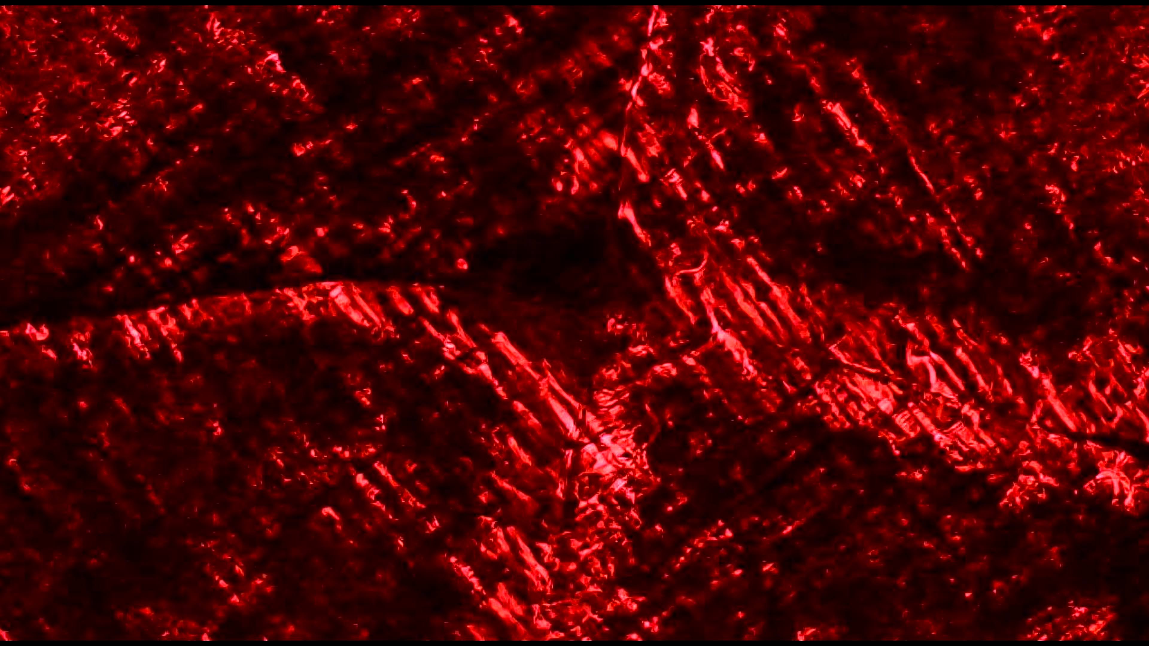
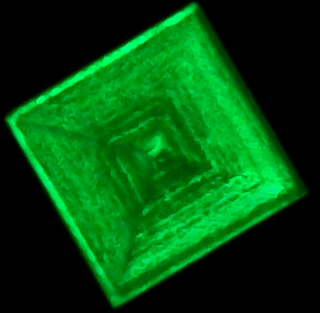
3.94 micron horizontal FOV NaCl salt crystal 640 nm red laser.
NanoFraction is initially targeting customers in the material sciences field, specifically industrial fabricators of carbon-based lattice substrates, i.e. diamond. NanoFraction aims to demonstrate that focusing on lattice substrates will lead to wider translational impacts in the semiconductor and biological markets. Microscopy at the super-resolution range and sensitivity is unlocking newly emerging areas of research. The NanoFraction DHOM system can be directly compared to fluorescent SRM and to transmission electron microscopy TEM but with no sample preparation or labeling needed.
Nanoscale imaging is an indispensable tool for research and discovery and is also required for production and quality assurance processes. In the semiconductor market, the need for next generation substrates with improved unit heat properties such as diamonds is a key driver of future growth. A key factor in yields is the inspection. Currently the only method for diamond wafer inspection is destructive testing which by definition lowers yields.
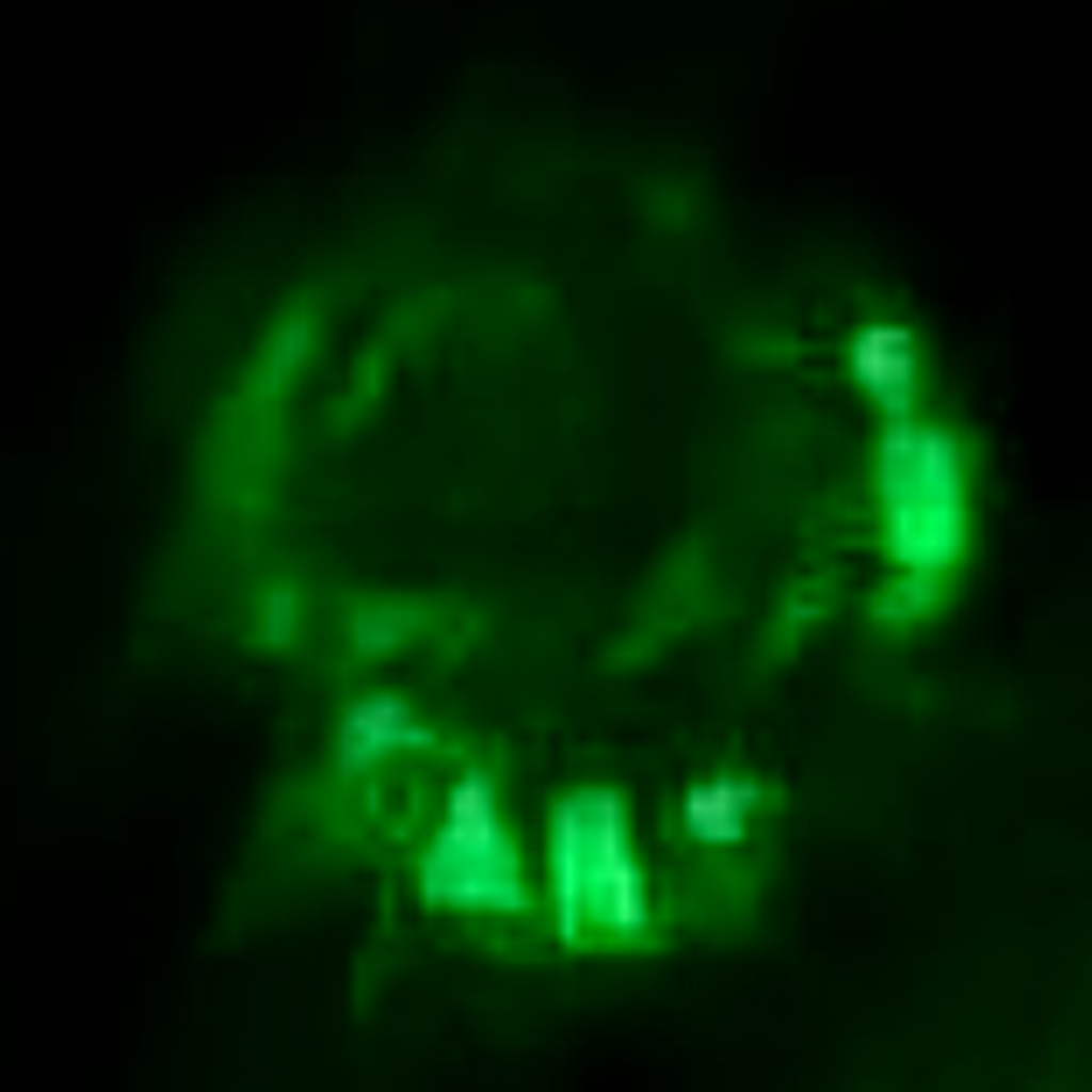
SARS-CoV-2 features captured by the DHOM system. SARS-CoV-2 is known to be smaller than the diffraction limit of 200nm, avg width being ~120nm. Captured image display features of theSARS-CoV-2 virion. Some features of the virion are focused at the bottom and right edges. Comparison with observations from the literature indicate the presence of SARS spikes(~14 nm). Morphology of SARS spike stem insertion through the wall(~7.8 nm) with the RNA of the virion can also be seen at the bottom edge.

First optical image of the SARS-CoV-2 virion captured by NF Jan, 2023.
Over the last 18 months, NanoFraction has conducted a number of experiments with several configurations of the optical circuit to develop a preliminary dataset of NaCl monomers via transmission and as well as C-4 diamond wafers via reflection at nanometric scales. NF is also collecting data on biological samples i.e. Sars-CoV-2 and Tobacco Mosaic Virus (TMV). All these experiments were added to data sets that have been used for basic validation, calibration, and correlation to the scientific model of the optical method. The experimental data were compared to TEM or theoretical data for validation. These images are also being used as input for training; a whole new generation of nanoscale AI models of the world.
The DHOM system uses lasers in the range of frequencies that go from violet to red (i.e. wavelengths ~ 400 nm up to ~ 700 nm) and acquire static and dynamic images in transmission and reflection of objects in the nanometer range. The method’s sensitivity is a function of the field of view. With a field of view of 3.9 micrometers, the current version of the DHOM has a resolution in the 10-2 nm range. The ratio of the field of view to resolution is on the order of magnitude of 3X10⁻⁶. When these results are compared against TEM, the DHOM is an optical microscope unique within these imaging capabilities.

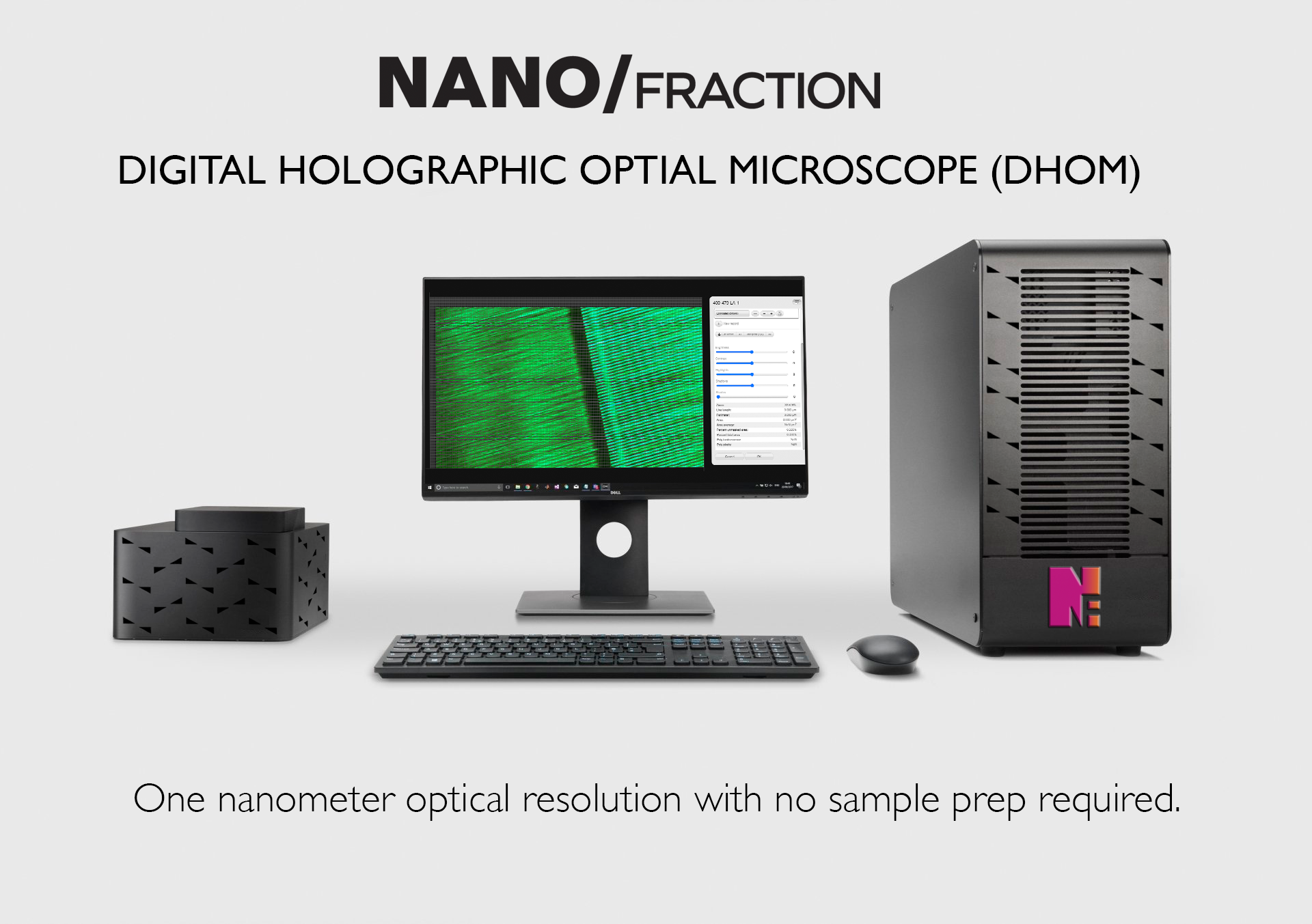
Mock ad for DHOM system (*not final design).
NanoFraction’s goal is to offer a line of Holographic DHOM systems with high-sensitivity resolution that is simple, robust and cost-effective to operate and maintain. Our instrumentation allows the scientist or researcher to investigate and validate their research with images free of chemical or temperature treatment which allows for visualizations in a wider range of environments.
NanoFraction is exploring a range of designs and configurations for the DHOM System. NanoFraction places a premium on product and interface design. We are not just focused on making the most sensitive optical capture instrument, but also want to take aesthetics and functionality into consideration. This design rigor also extends into the interface and software design. We are motivated to work in an open science framework so that our underlying work can be validated by the larger science community.
Below are design studies for our DHOM system. Further down this webpage, you will see a section called DATA. Here is where the real magic begins… you can see some of the data we have captured and experiment with it on your own. All our captured images can be easily viewed and analyzed in any web browser. This also goes for group sharing and co-analysis with multiple investigators. We are building a backend tool-chain to support nanoscopy research.


Design studies for NanoFraction DHOM System
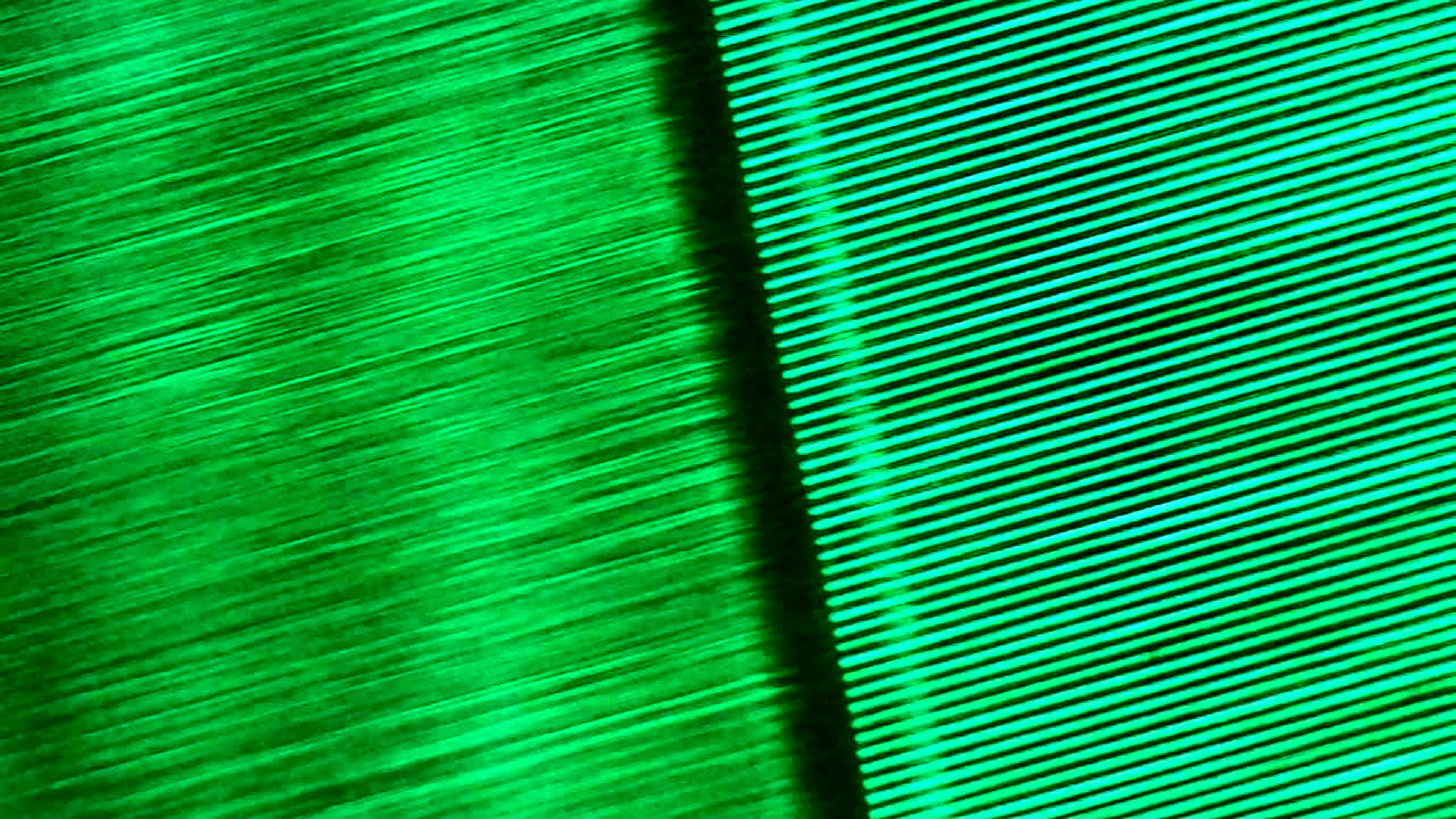
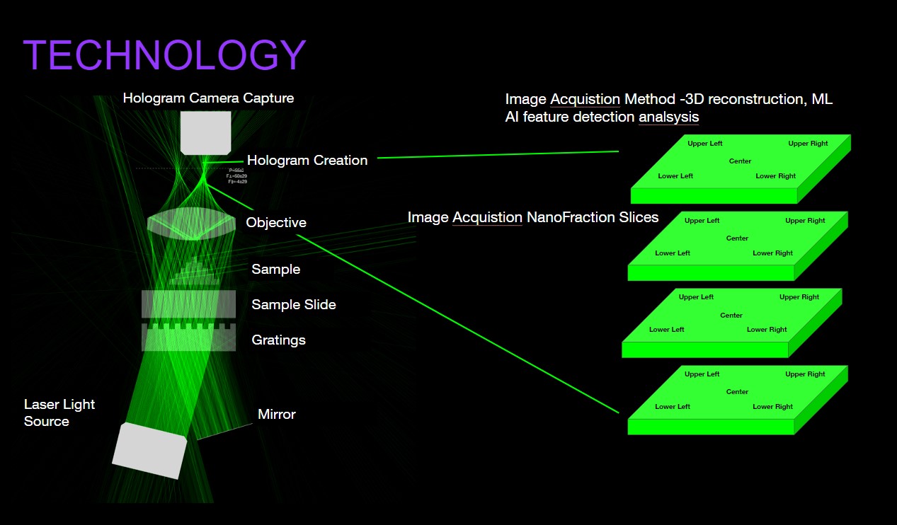
The foundations of the DHOM System are the same for reflection on a surface or transmission through a transparent media. Basic procedures, equations and software apply to both cases. A current POC is with Great Lakes Crystal Technologies (GLCT), a synthetic diamond manufacturer. The image below shows the optical setup used for sensing the defects of a thin diamond wafer. Using single illumination, it is possible to sense depth changes with respect to a reference plane,-. By using double illumination, it is possible to reconstruct the surface of the object.
In this section, synthetic diamond manufacturer Great Lakes Crystal Technologies (GLCT) has teamed with NanoFraction. The pace of technical progress for diamond electronic components for sensors and logic gates is dependent on the quality control inspection speed and quality. Diamond substrate is an important part of high powered computing as silicon transistors have reached a physical limit of heat per unit of compute. Given GLCT’s knowledge of the chemical vapor deposition (CVD) diamond growth process and NF’s highly sensitive, proprietary optical hardware and AI software analysis system, there is an opportunity to prove that NF’s Digital Holographic Optical Microscopy can provide a fast, low-cost inspection system for screening diamond seeds. This is significant for GLCT’s edge cases where current modalities of inspection cannot be scaled up for an in-process, in-house solution. In contrast, NF’s method can be integrated into an automated feedback control loop in a production process.

Current QC methods for diamond wafer growth are destructive, both growth time and resources are lost.
Capturing images of the diamond wafers with the DHOM system requires no sample preparation. Seeds can be placed individually or fed through an automated tray with a 5 x 5 wafer grid. NanoFraction's no sample preparation eliminates a significant amount of time required for current inspection methods and also cuts down the duration of the production process. NanoFraction’s method can be applied to seeds for the purpose of: Non-destructive technique to screen and weeding out bad seeds.

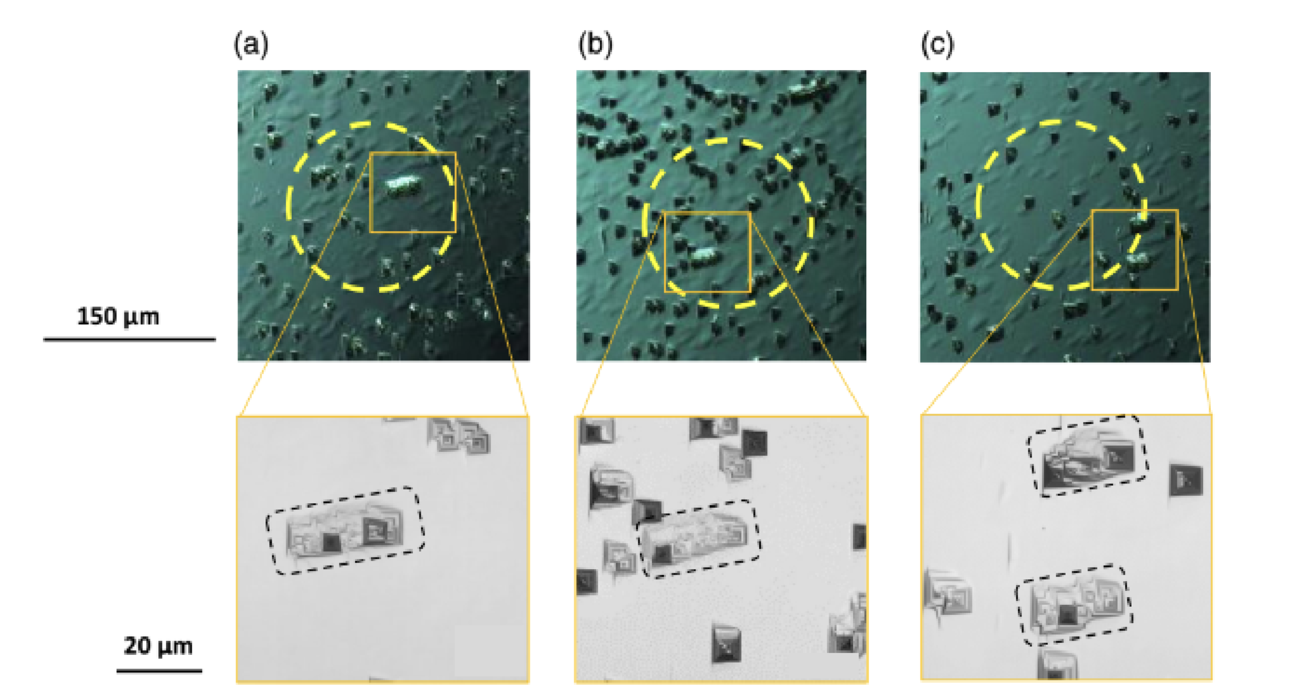
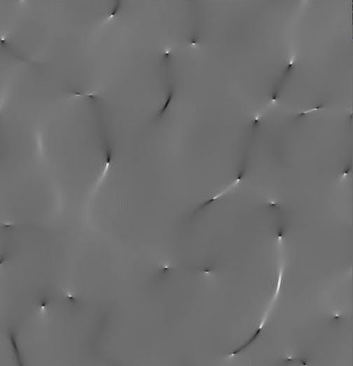
Image of diamond wafer captured with NF DHOM System.
In the following section called DATA, you can see a complete analysis of one diamond seed wafer. We begin by investigating the 3 mm x 3mm x 0.5 mm sample and 500 micron regions. Using our holographic data set and analysis software, we are able to reconstruct higher fidelity regions as we zoom onto the surface of the wafer. By zooming on regions of the order of 20 microns, we are able to pinpoint diamond dislocation on the surface to within 100 nm. This gives us the unprecedented capability to look for catastrophic dislocations that will contribute to a sub-par diamond wafer. The speed and detail of this analysis cannot be matched by any other SRM method.

Schematic of NF DHOM holographic optical circuit.
Acknowledgements
This work could not have been done without the financial support of General Stress Optics, Inc.and the scientific research and contributions by Cesar Sciammarella, Luciano Lamberti, and Federico Sciammarella. A special acknowledgement needs to be made to Esther Sciammarella for her dedicated support and encouragement in the face of many uncertain challenges. There is no way in which science can be done without the support of family and friends. What often is a treacherous path can not be traveled alone. These background efforts of support are the silent army of science.
NanoFraction Inc. is in the formative stages of pre-seed funding. A dedicated team of supporters in no particular order continue to push the thinking and doing of this for-profit private social enterprise. Thank-you to Ian Myles, Mike Brown, Thomas Grauman, Daniell Hebert, Brady Anderson, Norio Fujikawa, Richard Sportsman, Joseph Jackson, David K., Jenny Suh, and Matt Ewert.
NF would also acknowledge the support of MXD mxdusa.org, The Polytechnic of Bari, BioTech and Beyond, and Great Lakes Crystal Technologies.

Names: Sciammarella, Eduardo, 2023—Author. Sciammarella, Eduardo, 2023—Nanographer.
Title: Dawn of Optical Super-resolution, July 2023.
Description: NanoFraction, Inc. | San Diego, CA, 2023.
